Chapter 10 of 11
Revision Notes
Electronics and Communication — Revision Notes
Tamil Nadu Board · Class 12 · Physics
Electronics and Communication revision notes for Tamil Nadu Board Class 12 Physics: 4 topics in quick points. Includes Energy Band Diagram.
87 questions30 flashcards5 concepts
Interactive on Super Tutor
Studying Electronics and Communication? Get the full interactive chapter.
Quizzes, flashcards, AI doubt-solver and a step-by-step study plan — built for revision notes and more.
Free trial, no card needed.
Super Tutor
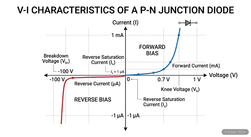
Learn better with visuals Super Tutor pairs illustrations like this with notes and quizzes for Electronics and Communication.
Key Topics to Revise
1
1. Energy Band Diagram and Classification of Materials
- Energy bands form when millions of atoms come together - valence and conduction bands are separated by forbidden energy gap (Eg)
- Insulators have large Eg (≈6 eV), electrons cannot jump to conduction band even with external field or temperature increase
- Conductors have overlapping valence and conduction bands, allowing free electron movement at all temperatures
2
2. Intrinsic and Extrinsic Semiconductors
- Intrinsic semiconductor: pure semiconductor where number of electrons (ne) = number of holes (nh), both at same level
- At 0K intrinsic semiconductor behaves like insulator, at higher temperature thermal energy creates electron-hole pairs
- Total current in intrinsic semiconductor: I = Ie + Ih (electron and hole currents)
3
3. P-N Junction Diode Formation and Characteristics
- P-N junction: contact surface between p-type and n-type semiconductor with single p-n junction
- Depletion layer: thin region free from mobile charge carriers (electrons and holes) near junction
- Formation mechanism: diffusion of majority carriers across junction (electrons from n to p, holes from p to n)
4
4. Rectification: Half-Wave and Full-Wave Rectifiers
- Rectification: conversion of alternating voltage/current to direct voltage/current using diodes
- Rectifier: device performing rectification function
- Half-wave rectifier: single diode, passes only positive (or negative) half cycle of AC input
Get complete notes with diagrams and examples
Full NotesKey Concepts
When atoms are brought close togetherPure semiconductors without any impuritiesDoping is the process of addingA pForward bias occurs when the positive
Frequently Asked Questions
What are the important topics in Electronics and Communication for Tamil Nadu Board Class 12 Physics?
Key topics in Electronics and Communication include Energy Band Diagram and Classification of Materials, Intrinsic and Extrinsic Semiconductors, P-N Junction Diode Formation and Characteristics, Rectification: Half-Wave and Full-Wave Rectifiers. Study these first, then practise questions on each for the Tamil Nadu Board Class 12 board exam.
How should I revise Electronics and Communication for the Tamil Nadu Board Class 12 board exam?
Learn the core ideas first, then work through the 87 practice questions on Electronics and Communication. Revise definitions regularly and use flashcards for quick recall before the exam.
Sources & Official References
Content is aligned to the official syllabus. Refer to the board website for the latest curriculum.
More resources for Electronics and Communication
For serious students
Get the full Electronics and Communication chapter — start free.
Quizzes, flashcards, an AI doubt solver and a study plan for Tamil Nadu Board Class 12 Physics. Free to start, no card needed.