Semiconductors and Semiconducting Devices — Concept Maps
NIOS · Class 12 · Physics
4 concept maps of Semiconductors and Semiconducting Devices for NIOS Class 12 Physics, each also written out as a text outline.
Interactive on Super Tutor
Studying Semiconductors and Semiconducting Devices? Get the full interactive chapter.
Quizzes, flashcards, AI doubt-solver and a step-by-step study plan — built for concept maps and more.
Free trial, no card needed.
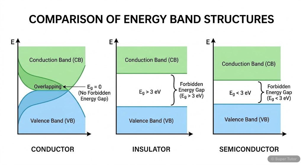
One of 12 illustrations for Semiconductors and Semiconducting Devices in Super Tutor — alongside flashcards, concept maps and practice questions.
Semiconductors and Semiconducting Devices - Concept Hierarchy
The map in words
- Semiconductors and Semiconducting Devices
- Energy Bands
- Valence Band
- Conduction Band
- Band Gap Energy
- Conductors
- Semiconductors
- Insulators
- Types of Semiconductors
- Intrinsic Pure
- Electron-hole pairs
- Room temperature
- Negative resistance coefficient
- Extrinsic Doped
- n-type Donor
- Group V dopants
- Electrons majority
- p-type Acceptor
- Group III dopants
- Holes majority
- n-type Donor
- Intrinsic Pure
- p-n Junction
- Depletion Region
- Width 0.5 micrometers
- Fixed ions
- No mobile carriers
- Barrier Potential
- Silicon 0.7V
- Germanium 0.3V
- Forward Bias
- Low resistance
- Large current mA
- Reverse Bias
- High resistance
- Small current nanoamperes
- Depletion Region
- Diodes
- Zener Diode
- Voltage regulation
- Reverse breakdown
- Light-Emitting Diode
- Electroluminescence
- Color by band gap
- Photodiode
- Light detection
- Photovoltaic effect
- Reverse bias operation
- Solar Cell
- Energy conversion
- Three processes
- Fourth quadrant plot
- Zener Diode
- Transistors
- Structure
- Three regions
- Two junctions
- Emitter Base Collector
- Types
- n-p-n transistor
- p-n-p transistor
- Configurations
- Common Emitter
- Highest gain
- Most used
- Common Base
- High frequency
- Common Collector
- Impedance match
- Common Emitter
- Characteristics
- Input characteristics
- Output characteristics
- Active region
- Saturation region
- Cutoff region
- Structure
- Energy Bands
Semiconductors and Semiconducting Devices — Complete Concept Map
The map in words
- Semiconductors
- Energy Bands
- Valence Band VB
- Conduction Band CB
- Band Gap
- Conductor Zero Gap
- Semiconductor Max 3 eV
- Insulator Over 3 eV
- Types of Semiconductors
- Intrinsic Pure
- Equal electrons and holes
- Si and Ge
- Negative temp coefficient
- Extrinsic Doped
- n-type
- Pentavalent dopant
- Electrons majority
- Donor impurity
- p-type
- Trivalent dopant
- Holes majority
- Acceptor impurity
- n-type
- Intrinsic Pure
- p-n Junction Diode
- Depletion Region
- Width 0.5 micron
- Barrier Si 0.7V Ge 0.3V
- Forward Bias
- Low resistance
- Current in mA
- Knee voltage
- Reverse Bias
- High resistance
- Leakage current
- Breakdown voltage
- Special Diodes
- Zener Voltage regulation
- LED Light emission
- Photodiode Light detection
- Solar Cell Light to electricity
- Depletion Region
- Transistors
- Structure
- Emitter Most doped
- Base Least doped Thinnest
- Collector Largest
- Types
- npn Arrow outward
- pnp Arrow inward
- Current Gain
- Alpha CB gain less than 1
- Beta CE gain greater than 1
- Configurations
- CE Most used
- CB Constant current
- CC Impedance matching
- Structure
- Energy Bands
Correct vs Incorrect Thinking: p-n Junction Concepts
The map in words
- Common Misconceptions
- Which Topic?
- Net Charge: Wrong: p-type is positive
- Holes exist BUT so do fixed negative acceptor ions
- Holes plus Acceptor Ions equals Zero Net Charge
- Holes exist BUT so do fixed negative acceptor ions
- Net Charge: Right: Both types are neutral
- At 0K: Wrong: Semiconductor still conducts
- No thermal energy means no carriers in conduction band
- Conductivity is exactly Zero at 0K
- No thermal energy means no carriers in conduction band
- At 0K: Right: Perfect insulator at 0K
- Reverse Bias: Wrong: Zero current flows
- Minority carriers are swept by reverse field
- Reverse saturation current: nA in Si, uA in Ge
- Minority carriers are swept by reverse field
- Reverse Bias: Right: Small leakage current flows
- Net Charge: Wrong: p-type is positive
- Which Topic?
Semiconductors and Semiconducting Devices
The map in words
- Semiconductors and Semiconducting Devices
- Energy Bands in Solids
- Types of Semiconductors
- p-n Junction
- Types of Diodes
- Transistors
Explore these maps interactively
Explore DiagramsFrequently Asked Questions
What are the important topics in Semiconductors and Semiconducting Devices for NIOS Class 12 Physics?
What do the concept maps for Semiconductors and Semiconducting Devices show?
How should I revise Semiconductors and Semiconducting Devices for the NIOS Class 12 board exam?
Sources & Official References
Content is aligned to the official syllabus. Refer to the board website for the latest curriculum.
More resources for Semiconductors and Semiconducting Devices
Practice Quiz
Test yourself with a quick quiz
Important Questions
Exam-style questions with answers
Revision Notes
Key points for last-minute revision
Formula Sheet
The chapter's formulas in one place
Chapter Summary
Understand the chapter at a glance
Study Plan
Step-by-step plan for this chapter
Flashcards
Quick-fire cards for active recall
Syllabus
What topics to cover
For serious students
Get the full Semiconductors and Semiconducting Devices chapter — start free.
Quizzes, flashcards, an AI doubt solver and a study plan for NIOS Class 12 Physics. Free to start, no card needed.