Semiconductors and Semiconducting Devices — Revision Notes
NIOS · Class 12 · Physics
Semiconductors and Semiconducting Devices revision notes for NIOS Class 12 Physics: 4 topics in quick points. Part of the NIOS Class 12 Physics syllabus.
Interactive on Super Tutor
Studying Semiconductors and Semiconducting Devices? Get the full interactive chapter.
Quizzes, flashcards, AI doubt-solver and a step-by-step study plan — built for revision notes and more.
Free trial, no card needed.
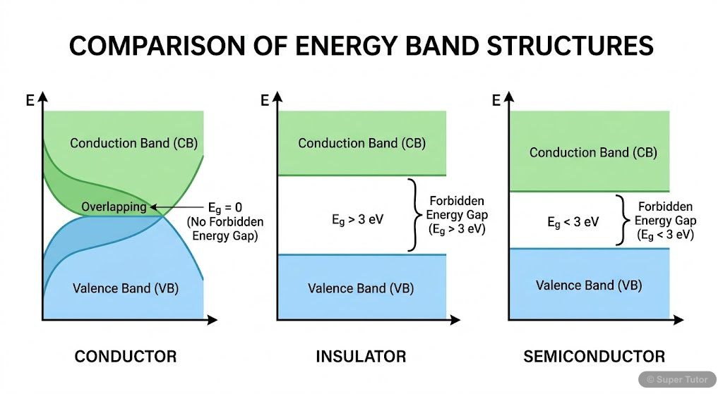
One of 12 illustrations for Semiconductors and Semiconducting Devices in Super Tutor — alongside flashcards, concept maps and practice questions.
Key Topics to Revise
Energy Bands and Classification of Solids
- In an isolated atom, electrons occupy discrete energy levels. When atoms come together in a solid, these levels broaden into energy bands due to interaction between atoms.
- In a solid with N atoms, each energy level splits into 2N closely spaced sub-levels forming a quasi-continuous energy band. The energy difference between adjacent sub-levels is approximately ΔE ≈ 10⁻²
- Two most important bands: Valence Band (VB) — formed from filled valence levels; Conduction Band (CB) — formed from unfilled energy levels.
Intrinsic and Extrinsic Semiconductors
- Intrinsic Semiconductor: A pure semiconductor with no added impurities. Example: Pure Si, Pure Ge.
- In an intrinsic semiconductor, electron-hole pairs are ALWAYS generated in equal numbers due to thermal energy: ni = ne = nh (intrinsic carrier concentration).
- At 300K: Ge has ni ≈ 2.5 × 10¹⁹ m⁻³; Si has ni ≈ 1.5 × 10¹⁶ m⁻³.
p-n Junction Formation and Barrier Potential
- A p-n junction is formed by doping one side of a single semiconductor crystal with acceptor impurities (p-side) and the other side with donor impurities (n-side).
- At the moment of junction formation: High concentration of electrons in n-region and holes in p-region causes DIFFUSION across the junction.
- Diffusion: Electrons move from n→p and holes move from p→n across the junction and RECOMBINE, eliminating free charge carriers near the junction.
Forward and Reverse Biased p-n Junction
- BIASING means applying an external voltage to the p-n junction. The way battery is connected determines the type of bias.
- FORWARD BIAS: Positive terminal of battery → p-side; Negative terminal → n-side. This REDUCES the barrier potential.
- In forward bias: Majority carriers are pushed toward the junction → depletion region NARROWS → current flows when forward voltage exceeds barrier potential (0.7V for Si, 0.3V for Ge).
Get complete notes with diagrams and examples
Full NotesKey Concepts
Frequently Asked Questions
What are the important topics in Semiconductors and Semiconducting Devices for NIOS Class 12 Physics?
How should I revise Semiconductors and Semiconducting Devices for the NIOS Class 12 board exam?
Sources & Official References
Content is aligned to the official syllabus. Refer to the board website for the latest curriculum.
More resources for Semiconductors and Semiconducting Devices
Practice Quiz
Test yourself with a quick quiz
Important Questions
Exam-style questions with answers
Formula Sheet
The chapter's formulas in one place
Chapter Summary
Understand the chapter at a glance
Concept Maps
See how topics connect
Study Plan
Step-by-step plan for this chapter
Flashcards
Quick-fire cards for active recall
Syllabus
What topics to cover
For serious students
Get the full Semiconductors and Semiconducting Devices chapter — start free.
Quizzes, flashcards, an AI doubt solver and a study plan for NIOS Class 12 Physics. Free to start, no card needed.