Semiconductor Electronics: Materials, Devices and Simple Circuits — NCERT Solutions
Madhya Pradesh Board · Class 12 · Physics
NCERT Solutions for Semiconductor Electronics: Materials, Devices and Simple Circuits, Madhya Pradesh Board Class 12 Physics: 6 textbook questions solved.
Interactive on Super Tutor
Studying Semiconductor Electronics: Materials, Devices and Simple Circuits? Get the full interactive chapter.
Quizzes, flashcards, AI doubt-solver and a step-by-step study plan — built for NCERT solutions and more.
Free trial, no card needed.
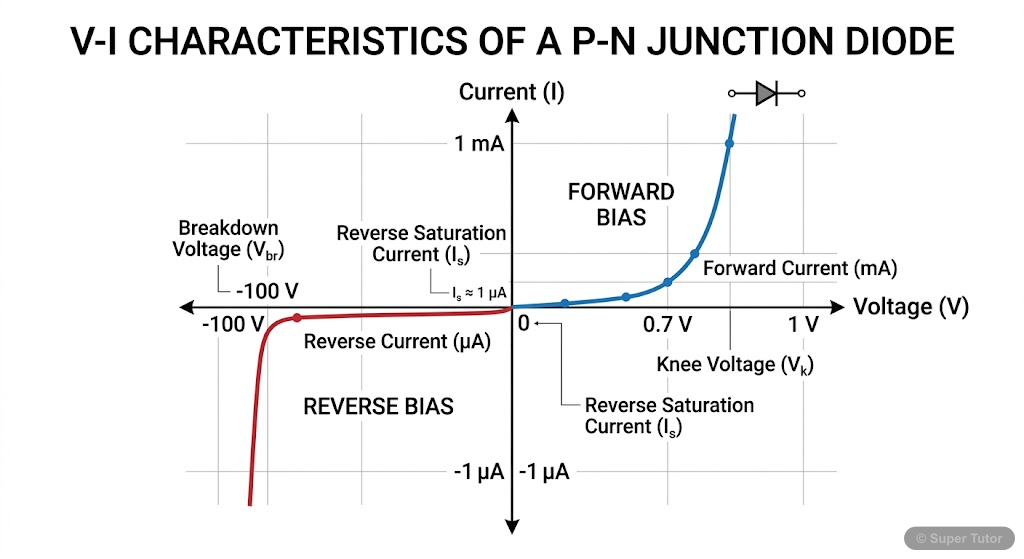
Learn better with visuals Super Tutor pairs illustrations like this with notes and quizzes for Semiconductor Electronics: Materials, Devices and Simple Circuits.
The first 3 solutions are open to read. The other 3 are free with a Super Tutor account.
Exercises
14.1In an n-type silicon, which of the following statement is true:
(a) Electrons are majority carriers and trivalent atoms are the dopants.
(b) Electrons are minority carriers and pentavalent atoms are the dopants.
(c) Holes are minority carriers and pentavalent atoms are the dopants.
(d) Holes are majority carriers and trivalent atoms are the dopants.Show solution
Correct Option: (c) Holes are minority carriers and pentavalent atoms are the dopants.
Justification:
In an n-type semiconductor, silicon (tetravalent) is doped with pentavalent atoms (donors) such as As, Sb, or P. Each dopant atom donates one extra electron to the conduction band. Therefore:
- Electrons are the majority carriers.
- Holes are the minority carriers.
- The dopants are pentavalent atoms.
Option (a) is wrong because it states trivalent atoms are dopants (that would give p-type). Option (b) is wrong because electrons are majority carriers, not minority. Option (d) is wrong because holes are not majority carriers in n-type.
Hence, option (c) is correct.
14.2Which of the statements given in Exercise 14.1 is true for p-type semiconductors?Show solution
Correct Option: (d) Holes are majority carriers and trivalent atoms are the dopants.
Justification:
In a p-type semiconductor, silicon (tetravalent) is doped with trivalent atoms (acceptors) such as B, Al, or In. Each dopant atom creates a hole (electron vacancy) in the valence band. Therefore:
- Holes are the majority carriers.
- Electrons are the minority carriers.
- The dopants are trivalent atoms.
This matches statement (d) from Exercise 14.1, which is the correct answer for p-type semiconductors.
14.3Carbon, silicon and germanium have four valence electrons each. These are characterised by valence and conduction bands separated by energy band gap respectively equal to , and . Which of the following statements is true?
(a)
(b)
(c)
(d) Show solution
Correct Option: (c)
Given/Known values:
- (Carbon/Diamond — insulator)
- (Silicon — semiconductor)
- (Germanium — semiconductor)
Concept: As we go down Group 14 of the periodic table (C → Si → Ge), the atomic size increases, the outermost electrons are farther from the nucleus, and the interatomic bonding becomes weaker. This results in a decrease in the energy band gap.
Conclusion:
Hence, option (c) is correct.
(a) free electrons in the n-region attract them.
(b) they move across the junction by the potential difference.
(c) hole concentration in p-region is more as compared to n-region.
(d) All the above.
Free with a Super Tutor account
(a) raises the potential barrier.
(b) reduces the majority carrier current to zero.
(c) lowers the potential barrier.
(d) None of the above.
Free with a Super Tutor account
Free with a Super Tutor account
3 more solved questions in Semiconductor Electronics: Materials, Devices and Simple Circuits
They are free with a Super Tutor account, along with practice quizzes and flashcards for this chapter. Free to start, no card needed.
Frequently Asked Questions
What are the important topics in Semiconductor Electronics: Materials, Devices and Simple Circuits for Madhya Pradesh Board Class 12 Physics?
Are these NCERT Solutions for Semiconductor Electronics: Materials, Devices and Simple Circuits free?
How should I revise Semiconductor Electronics: Materials, Devices and Simple Circuits for the Madhya Pradesh Board Class 12 board exam?
Sources & Official References
Content is aligned to the official syllabus. Refer to the board website for the latest curriculum.
More resources for Semiconductor Electronics: Materials, Devices and Simple Circuits
Practice Quiz
Test yourself with a quick quiz
Important Questions
Exam-style questions with answers
Revision Notes
Key points for last-minute revision
Formula Sheet
The chapter's formulas in one place
Chapter Summary
Understand the chapter at a glance
Concept Maps
See how topics connect
Study Plan
Step-by-step plan for this chapter
Flashcards
Quick-fire cards for active recall
Syllabus
What topics to cover
For serious students
Get the full Semiconductor Electronics: Materials, Devices and Simple Circuits chapter — start free.
Quizzes, flashcards, an AI doubt solver and a study plan for Madhya Pradesh Board Class 12 Physics. Free to start, no card needed.