Applications of Semiconductor Devices — Practice Quiz
NIOS · Class 12 · Physics
Try a 4-question quiz on Applications of Semiconductor Devices for NIOS Class 12 Physics: tap an answer to check it and see why.
Interactive on Super Tutor
Studying Applications of Semiconductor Devices? Get the full interactive chapter.
Quizzes, flashcards, AI doubt-solver and a step-by-step study plan — built for practice quiz and more.
Free trial, no card needed.
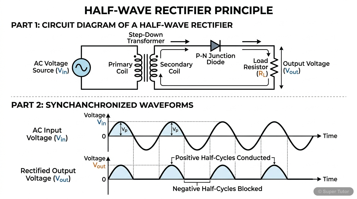
One of 4 illustrations for Applications of Semiconductor Devices in Super Tutor — alongside flashcards, concept maps and practice questions.
Quick Quiz: Applications of Semiconductor Devices
0/4Tap an answer to check it instantly. No sign-up needed for these 4.
In a half-wave rectifier, the peak ac voltage is 10 V. What is the dc output voltage (V_dc) across the load resistance?
In a full-wave rectifier, the peak ac voltage is 10 V. What is the dc output voltage (V_dc)?
A Zener diode with breakdown voltage 6 V is connected in a regulator circuit. The input voltage is 12 V and the series resistance R_s is 60 Ω. What is the current through R_s?
Which of the following is the correct Boolean expression for the output of a NAND gate with inputs A and B?
Sample Questions
In a common emitter (CE) transistor amplifier, the voltage gain A_V is given by which formula?
Show answer
A_V = –β × R_L / r_i
Step 1: In CE amplifier, the change in collector current is Δi_c = β × Δi_b. Step 2: Output voltage change is Δv_0 = –Δi_c × R_L (negative because increase in collector current reduces V_CE). Step 3: Input voltage v_s = Δi_b × r_i, so A_V = v_0/v_s = –β × R_L / r_i. The negative sign indicates 180° phase shift between input and output. β × r_i / R_L reverses the fraction. R_L / r_i misses the β factor.
In a CE amplifier, R_L = 2000 Ω, r_i = 500 Ω and β = 50. What is the magnitude of voltage gain?
Show answer
200
Step 1: Use the formula |A_V| = β × R_L / r_i. Step 2: Substitute values: |A_V| = 50 × 2000 / 500. Step 3: |A_V| = 100000 / 500 = 200. So the voltage gain magnitude is 200. Option 25 results from dividing β by R_L/r_i instead of multiplying. Option 100 is half the correct value (common error of using R_L/r_i without β). Option 50 is just the value of β.
Which logic gate gives output '1' ONLY when both inputs are '0'?
Show answer
NOR gate
Step 1: NOR = NOT + OR. Step 2: OR gate gives '1' when at least one input is '1'. Step 3: Inverting the OR output: NOR gives '1' only when OR output is '0', which happens only when BOTH inputs are '0'. AND gate gives '1' only when both inputs are '1'. OR gate gives '1' when at least one input is '1'. NAND gate gives '0' only when both inputs are '1' (i.e., output is '1' for all other combinations).
In a transistor switch circuit, when V_BB = 0 V (input is LOW), what is the state of the transistor and the output voltage V_0?
Show answer
Transistor is cut off; V_0 = V_CC
Step 1: When V_BB = 0, the base current I_B = –V_BE / R_B, which is negative (no forward bias). Step 2: Since I_B < 0, the transistor does not conduct and is in the CUT-OFF region. Step 3: Since no collector current flows, there is no voltage drop across R_L, so the entire supply voltage V_CC appears at the output. This is like an open switch – no current means full voltage at output. Saturation occurs only when V_BB is high enough to drive sufficient base current.
+41 more questions on Applications of Semiconductor Devices (NIOS Class 12 Physics)
Practise AllFrequently Asked Questions
What are the important topics in Applications of Semiconductor Devices for NIOS Class 12 Physics?
How many practice questions are there for Applications of Semiconductor Devices?
Sources & Official References
Content is aligned to the official syllabus. Refer to the board website for the latest curriculum.
More resources for Applications of Semiconductor Devices
Important Questions
Exam-style questions with answers
Revision Notes
Key points for last-minute revision
Formula Sheet
The chapter's formulas in one place
Chapter Summary
Understand the chapter at a glance
Concept Maps
See how topics connect
Study Plan
Step-by-step plan for this chapter
Flashcards
Quick-fire cards for active recall
Syllabus
What topics to cover
For serious students
Get the full Applications of Semiconductor Devices chapter — start free.
Quizzes, flashcards, an AI doubt solver and a study plan for NIOS Class 12 Physics. Free to start, no card needed.