Applications of Semiconductor Devices — Revision Notes
NIOS · Class 12 · Physics
Applications of Semiconductor Devices revision notes for NIOS Class 12 Physics: 4 topics in quick points. Part of the NIOS Class 12 Physics syllabus.
Interactive on Super Tutor
Studying Applications of Semiconductor Devices? Get the full interactive chapter.
Quizzes, flashcards, AI doubt-solver and a step-by-step study plan — built for revision notes and more.
Free trial, no card needed.
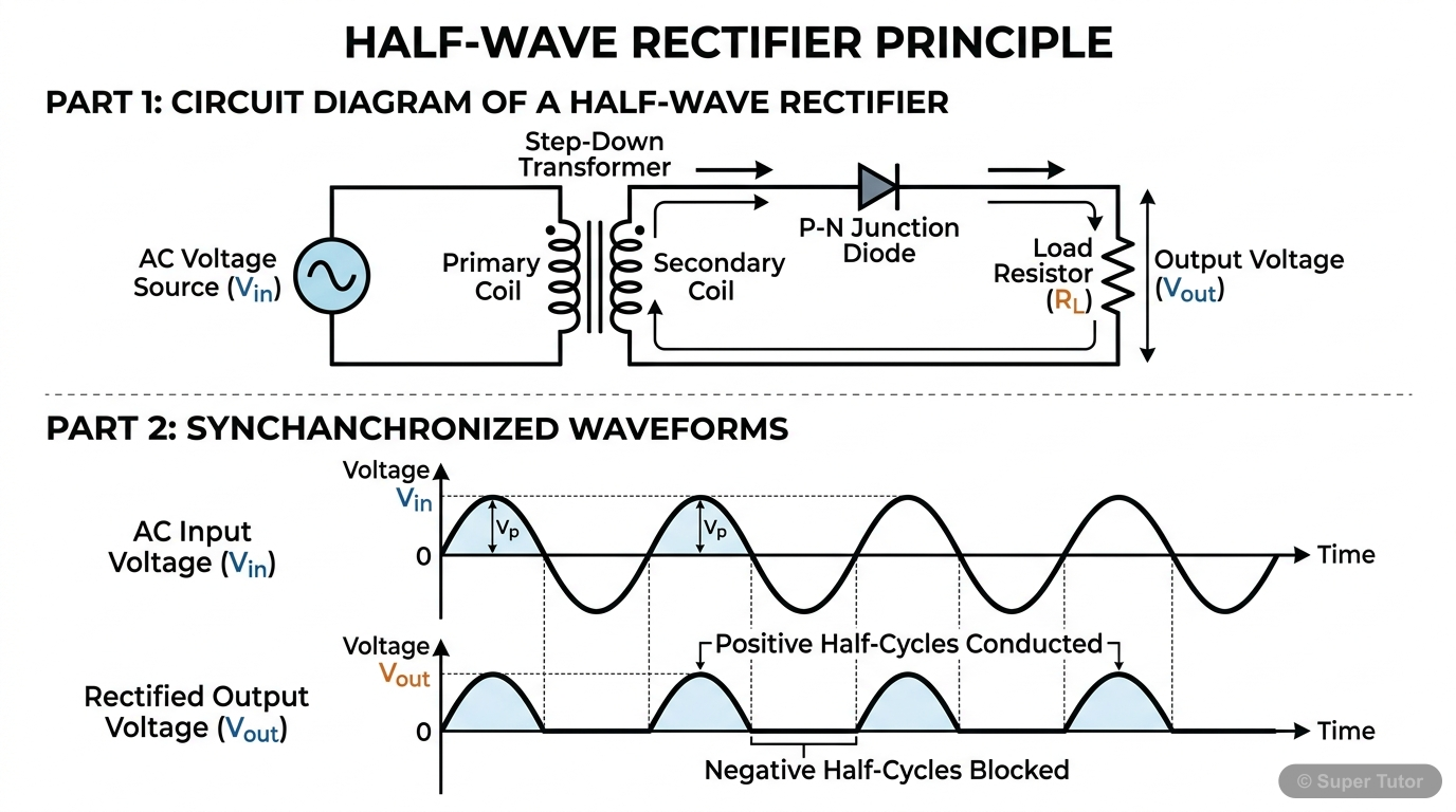
One of 4 illustrations for Applications of Semiconductor Devices in Super Tutor — alongside flashcards, concept maps and practice questions.
Key Topics to Revise
p-n Junction Diode as a Rectifier
- Rectification is the process of converting alternating current (AC) into direct current (DC).
- A p-n junction diode conducts only in forward bias, making it ideal for rectification.
- Half-wave rectification uses ONE diode – only one half-cycle (positive or negative) of AC passes through.
Zener Diode as a Voltage Regulator
- A Zener diode is a specially doped p-n junction designed to operate in the reverse breakdown region safely.
- Once reverse breakdown voltage (V_z) is reached, voltage across Zener remains nearly constant even if current changes — this is the principle of voltage regulation.
- The Zener diode is always connected in REVERSE BIAS in a regulator circuit.
Transistor as an Amplifier
- An amplifier increases the level (amplitude) of a weak input signal using energy from an external DC power source.
- The most common configuration is the Common Emitter (CE) mode using an n-p-n transistor.
- The collector is reverse biased (through R_L by battery V_CC) and the base is forward biased (by V_BB).
Transistor as a Switch
- A transistor can act as a switch by operating in its two extreme non-linear regions: Cut-off and Saturation.
- CUT-OFF region: Base current I_B = 0 (or negative). Transistor does not conduct. Collector current I_C ≈ 0. Output voltage V_CE = V_CC (switch is OFF).
- SATURATION region: Base current I_B > saturation value. Transistor conducts fully. V_CE ≈ 0. Collector current I_C = V_CC/R_L (switch is ON). Output voltage V_0 ≈ 0.
Get complete notes with diagrams and examples
Full NotesKey Concepts
Frequently Asked Questions
What are the important topics in Applications of Semiconductor Devices for NIOS Class 12 Physics?
How should I revise Applications of Semiconductor Devices for the NIOS Class 12 board exam?
Sources & Official References
Content is aligned to the official syllabus. Refer to the board website for the latest curriculum.
More resources for Applications of Semiconductor Devices
Practice Quiz
Test yourself with a quick quiz
Important Questions
Exam-style questions with answers
Formula Sheet
The chapter's formulas in one place
Chapter Summary
Understand the chapter at a glance
Concept Maps
See how topics connect
Study Plan
Step-by-step plan for this chapter
Flashcards
Quick-fire cards for active recall
Syllabus
What topics to cover
For serious students
Get the full Applications of Semiconductor Devices chapter — start free.
Quizzes, flashcards, an AI doubt solver and a study plan for NIOS Class 12 Physics. Free to start, no card needed.